
1st December 2021
I've been super busy doing a lot of repairs over the last few months. But a lot of them were either quick (and thus not very interesting)
or took 1-2 months to fix and I'm not sure I feel like writing up such a huge repair log hehe! Fortunately something came along recently that was
interesting and didn't take too long to fix.
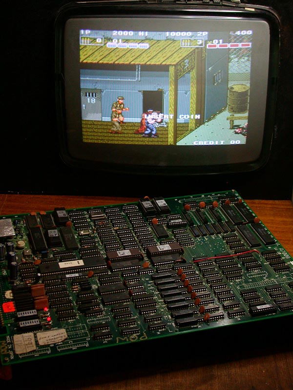
Check the board below.....

This came from a local friend who purchased this board along with a bunch of other stuff from someone who had a bunch of old arcade crap in
storage. It's a P.O.W. made in about 1988 by SNK. Normally POW has a sub board filled with 16 ROMs but this particular revision is a later
one that has 4x 4Mbit mask ROMs on the main board and no sub board. The rest of the ROMs are the same as older ROM archives. The interesting
thing about this board is that it was only just dumped back in December last year. So this version remained undumped for 33 years!! Also
note the 2 red wire mods appear to be factory mods. The very small one near the 24MHz oscillator is correcting a routing error to fix a
sync related problem.
The board is working but has a graphical fault where there are vertical lines across the entire screen.....
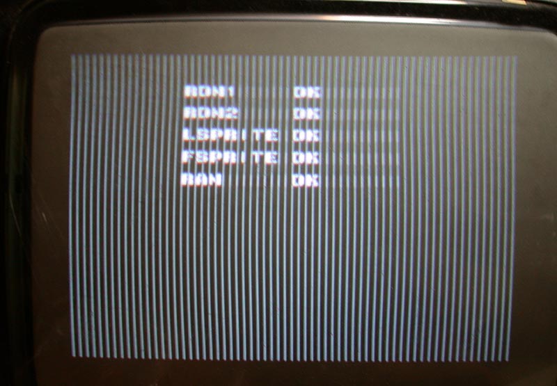
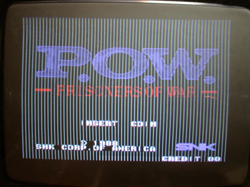
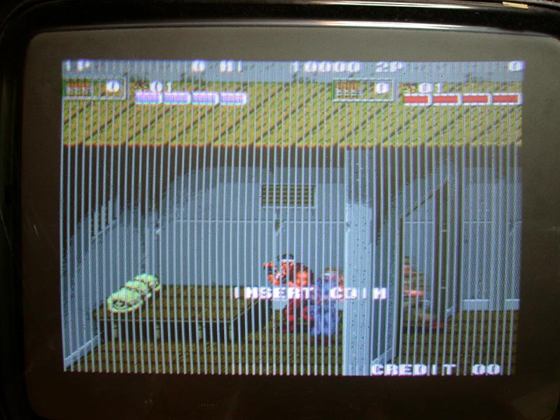
Of course the first thing to look at is RAM, but in this case there were no faults with the RAM. The start-up POST checks the main RAM,
LSPRITE RAM and FSPRITE RAM as well as the main program ROMs. All of those were good. The LSPRITE RAM is a bank of 3x Toshiba TMM2063 8k x8-bit
static RAMs. I would bet money that at least one of these RAMs is bad (they are a common failed chip on most late 80's and early 90's
Taito boards), but they test ok so they must be good. The FSPRITE RAM is a single 2016 2k x8-bit static RAM and is also good. The large bank
of RAMs at the bottom are for the sprites and since the player characters looked ok that RAM must bo ok too. I initially suspected the
larger (sprite) ROMs because this game doesn't use background data ROMs. Everything seems to be in the sprite ROMs which is very unusual. I
removed a couple of the ROMs and read them but they matched the MAME archive. I tested the game without those ROMs plugged in and there were
large chunks of graphics missing but the lines were still showing. Then I checked the text layer ROMs DG9 and DG10 but they also matched
MAME archives. I removed both ROMs and all the graphics disappeared and the lines also disappeared. On closer inspection it appears the
lines are on top of everything so they are actually on the text layer, meaning either DG9 or DG10 is causing the issue, but it's not the
actual ROMs. Lines usually mean missing data (either from a ROM or RAM) but the RAM/ROM tested ok so the fault had to be related to the
data being read from the text layer ROMs.
Unfortunately there are no schematics for this board so I spent about an hour and piggybacked a working logic chip on all the chips in the
same area as those ROMs. The only chip that had any affect on the lines was a 74LS157 at location K25. The lines went from being solid to
completely disappearing but it also affected everything on the text layer and a lot of it was also missing. Let's have a quick look how this chip
works.....

Looking at the function table we can see how the pins need to be set up and how the chip outputs the data.
Pin 15 (Strobe) must be low.
Pin 1 (A/B) can be low or high
A and B are the inputs (4 sets)
Y is the output (x4)
On this chip Strobe was low so that was ok. If it was high the chip essentially ignores all the inputs and outputs nothing. Select A/B was
low. This means that the A inputs are passed through to the Y outputs and the B inputs are ignored. If A/B was high, the opposite happens
where the B inputs are passed to the Y outputs and the A inputs are ignored. All of the A and B inputs were active and all outputs were also
active so the chip looked ok. I removed it and tested it out of circuit using my IC tester but it passed all tests. However this chip
is a key part of the (eventual) solution......
I piggybacked a working 74LS157 chip over the top and when held _just_ right, the lines disappeared! But the rest of the text layer was
corrupted or missing....

I eventually realised that it was a partially or un-connected A/B select pin that was causing that. I bent out pin 1 (A/B Select) so it
didn't touch the original chip and the text layer was completely missing. When held low the fault was the same as before. When held high the
whole screen inverted (i.e. flip screen). That pin is connected to some other logic that connects to the DIP switch for Flip Screen. While
not the solution, it's still interesting to see that the fault is the same even when the screen is flipped :-)
I traced the board and looked for where the A inputs were coming from. I found they were connected to 4x 74LS194 chips at locations J24,
J25, J26 and K26.
Now let's have a look at the datasheet for the 74LS194. The function table is shown on the 2nd page but studying it isn't required....
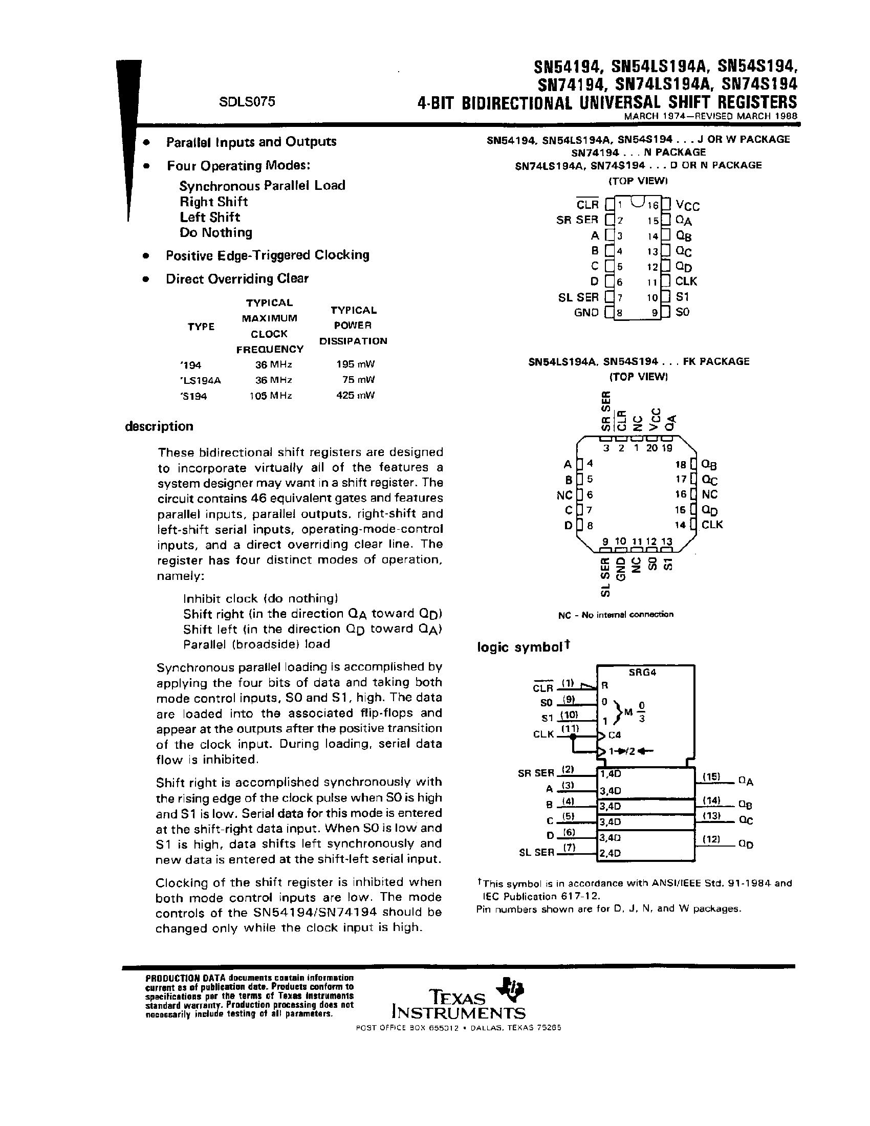
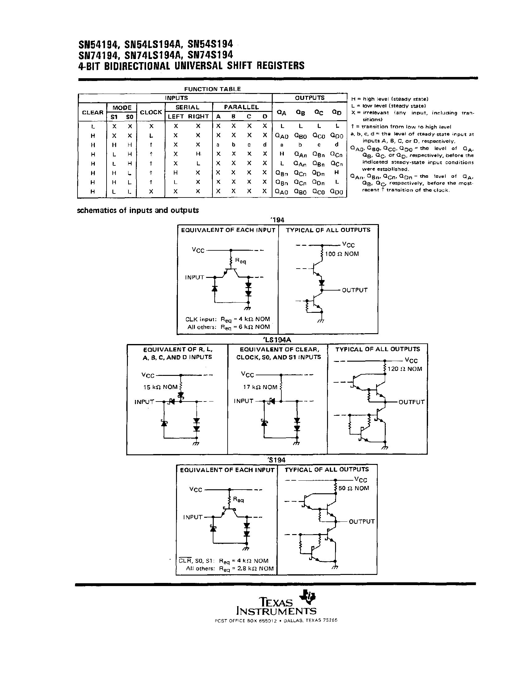
This chip is fairly complicated, but the important thing here is that there are 4 inputs and 4 outputs. If the inputs are active and the
clear and mode pins are set correctly the outputs should also be active. I checked the input pins (A, B, C, D) and output pins (QA, QB, QC,
QD) on all 4x 74LS194 chips with my logic probe and they were all active EXCEPT pin 3 on the 74LS194 at location J26. That pin (3) was
totally dead with NO activity!! This pin is an input. I tried to trace pin 3 and a section of the trace that was visually connected to pin 3
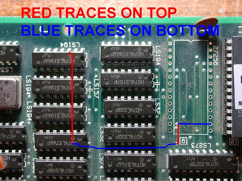
but it wasn't connected to anything so there's obviously a broken trace somewhere. I fully traced how the inputs on the 4x 74LS194 chips
were connected (except for pin 3 of the 74LS194 at J26) and I noticed a pattern.....

Now check the pinout of the 27C256 ROM.....
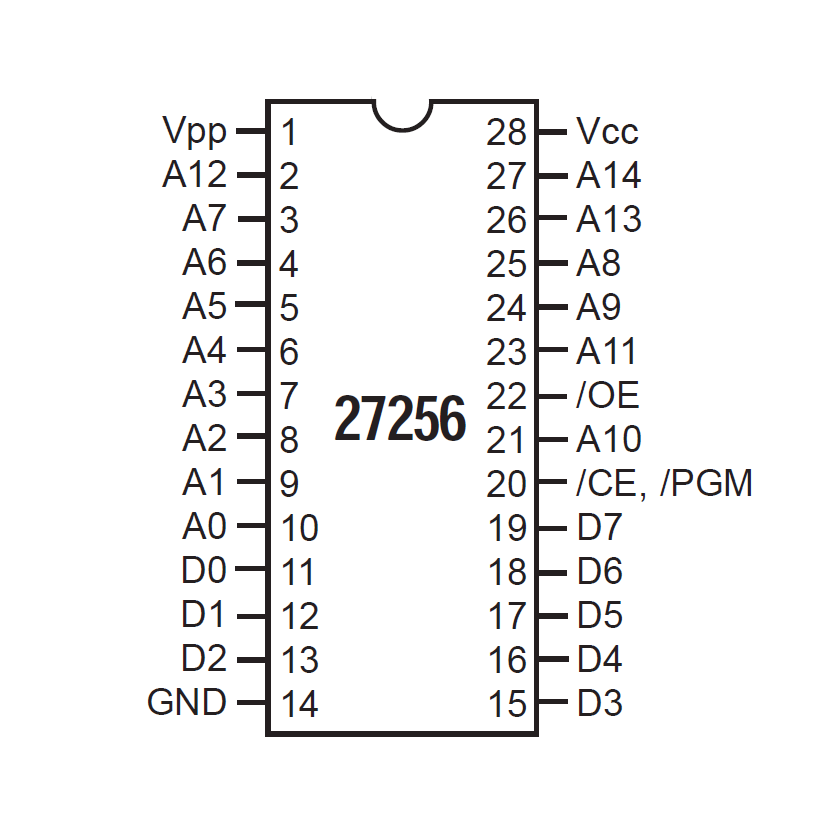
From the trace and EPROM pinout we can clearly see the broken trace leading to pin 3 comes from ROM DG9 pin 16 (D4). The fix is relatively
easy now but since there are no schematics I will have to look at the PCB and trace that track manually. But first I verified the connection by
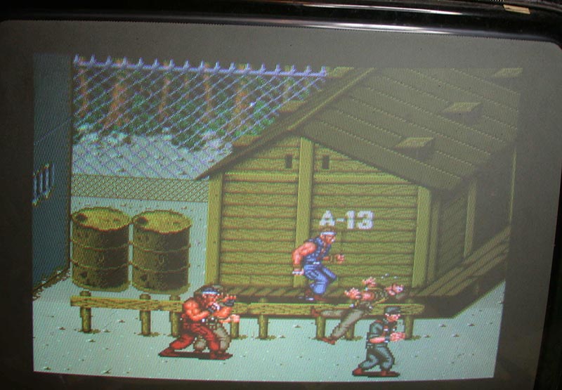
hooking up some micro-clips from the 74LS194 at J26 pin 3 to the DG9 ROM pin 16 and this is what I saw....

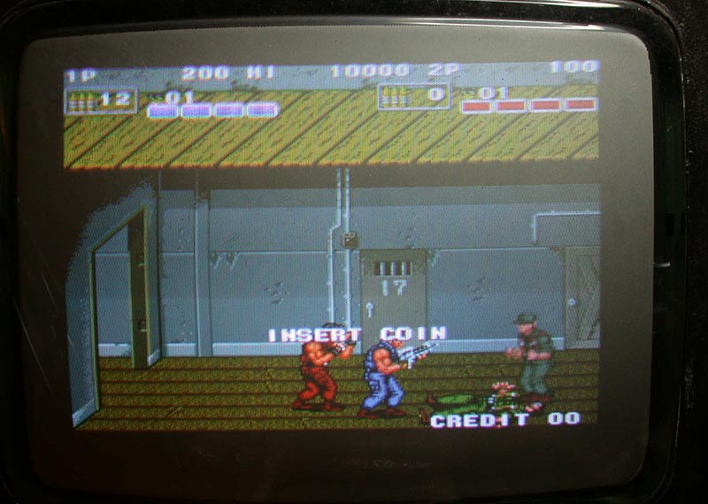
YUP! That's fixed alright hehe!
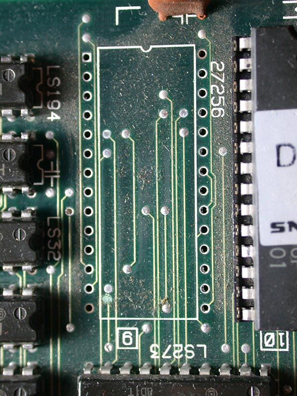
I traced the PCB manually and the track goes through a few vias. I checked the vias top and bottom for continuity because open vias are
often a problem, but usually in more modern PCBs with very tiny vias. In this case the vias were ok. Everything was connected except one
tiny trace going under the ROM socket but it wasn't visible even with the ROM removed. I had to remove the socket to see what was going
on. This is how the trace is routed on the PCB....
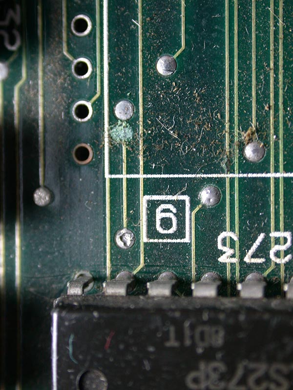
WOW! There's a tiny spot of water corrosion on the trace just at the bottom left edge where the socket was and it's eaten that trace and
caused a break!
Looking at the bottom of the ROM socket shows that the water was held there under the socket support pad and after many years the trace was
eaten away exactly at that point. I cleaned up the mess, patched the trace with a tiny piece of wire, cut off that little support pad and
put back the ROM socket, plugged in the ROM and powered on and the problem is now fixed permanently.
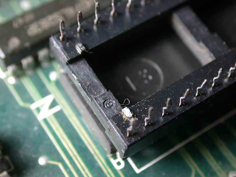


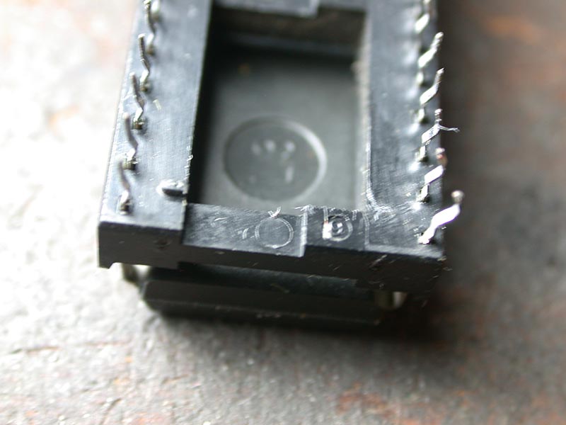

You can't even tell this has been fixed :-)
The unanswered question is how did that tiny dot of water get under the socket? That's a mystery that
probably even the original owner couldn't answer. At least now it's fully working and I'm sure the current owner will be very happy about
that. It wasn't that easy to fix this random fault but this proves with some determination and thinking, things can be fixed even without schematics :-
D
The take-away from this is always keep your boards clean and dry because water kills boards!
14th March 2021
I've been very busy over the last few months doing a lot of repairs and I am still very busy with more repairs banked up. Over the next few
weeks I will try to write up some of the more interesting ones here.
Here's the first one.... Toaplan Outzone.
It was working ok but had lines through the background graphics and a strange brown or green color band across the screen which moved when
sprites from the player were showing on screen....

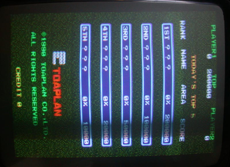

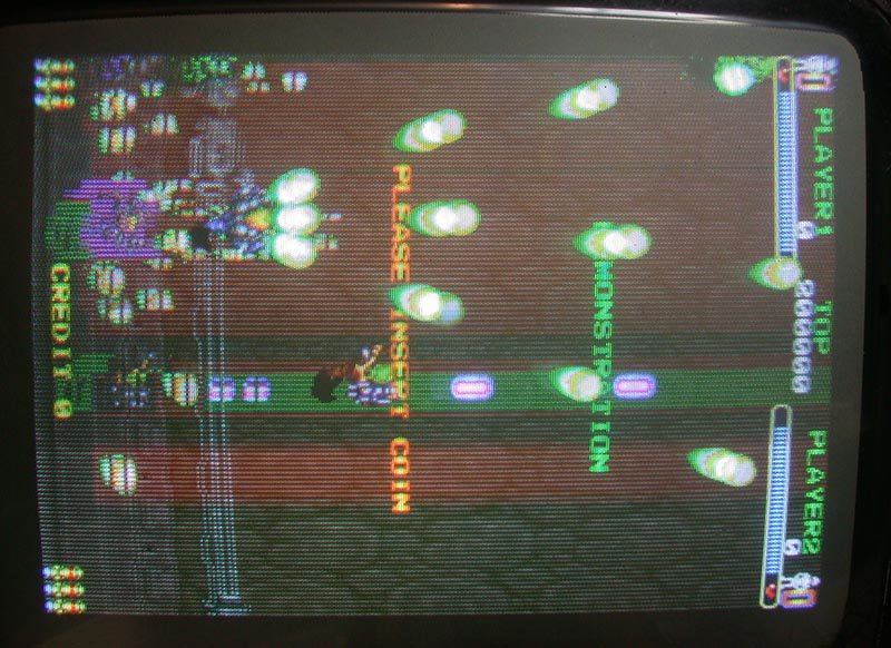
On any PCB one of the first things to check is the ROMs but there was a small issue. These are 1Mbit 28 pin mask ROMs so they have a non-standard
pinout that is not supported by any EPROM programmer. Of course being a dumping Guru I have an adapter to read them out but even so,
old mask ROMs can be flakey and I wanted to replace them with standard EPROMs. I pulled them and read them and they matched the MAME
archive. Since they were soldered in I added sockets so I could change them to EPROMs. Fortunately this PCB is set up to handle EPROMs
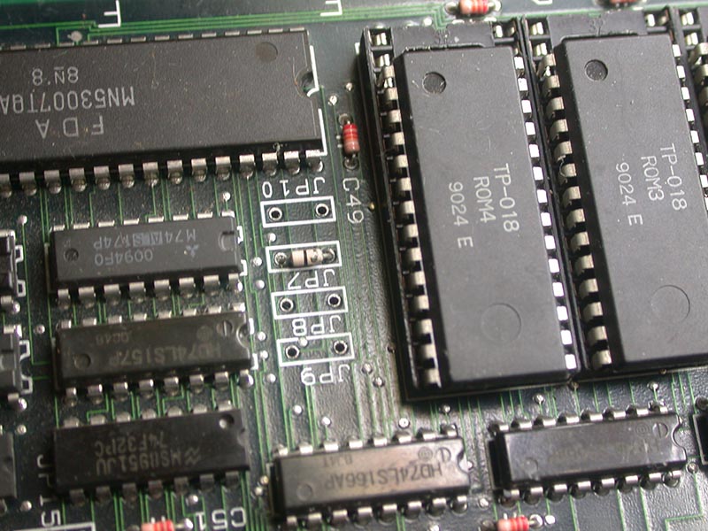
simply by adjusting some jumpers. Here's what they look like now, only JP7 is shorted for use with 28 pin mask ROMs....
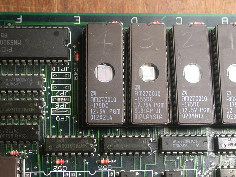
For standard 27C010 EPROMs the jumper needs to be moved to JP8 and another one added to JP9....
Unfortunately nothing changed on screen but at least now I know the ROMs are ok.
The next thing to check is the RAM so I spent some time piggy-backing some RAMs, but with limited success. When I piggybacked one specific
RAM the background graphics seemed to almost fix itself when powering off/on, but only occasionally....

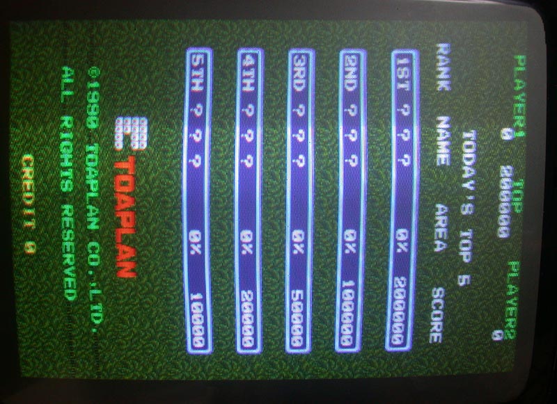
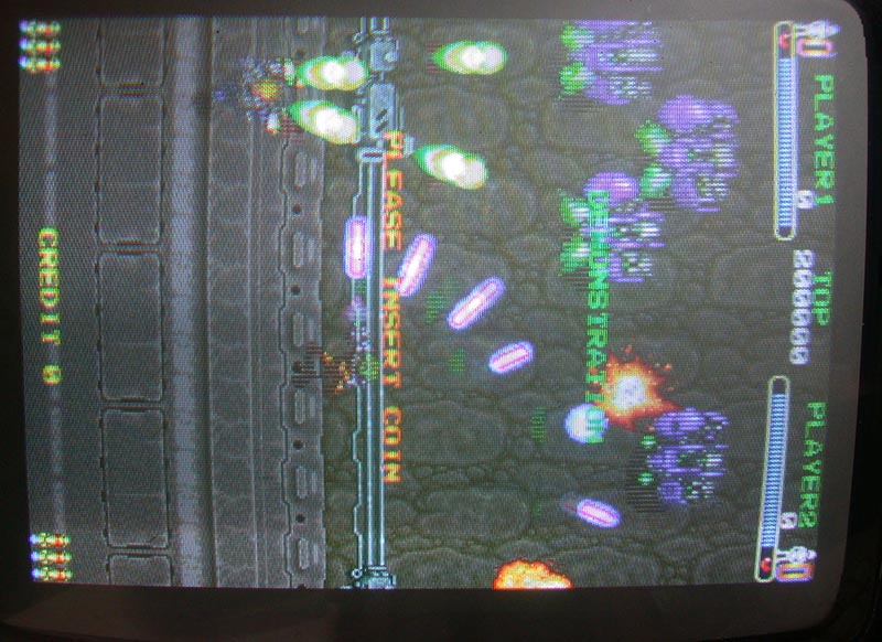
Notice the background on the high score screen is almost fixed... some black glitched text appears beside the green text and in game the
background is fixed and the strange band that appeared across the screen is gone but now another issue has appeared, the sprites have lines
through them! It's not shown in the pics, but the O.U.T.Z.O.N.E letters that fly in on the title screen also had lines through them when
they were moving.
The 'fix' seemed significant enough to warrant removing and replacing that RAM so I changed it for a known good
RAM...
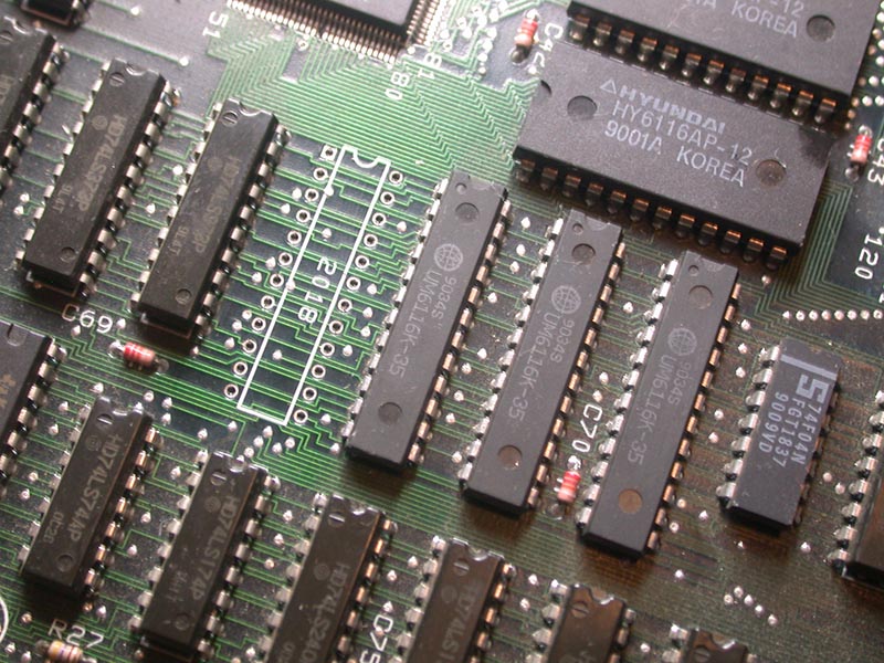
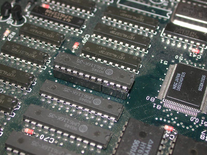
When powering on the exact same original fault showed with lines through the background, urggh!
OK, so no easy fix. It's time to get serious heh!
I probed that RAM with my logic probe and noticed that pin 17 had no activity. This is one of the data lines and should be always active so
it appears there's a broken trace somewhere. Looking at the pinout shows it is D7....
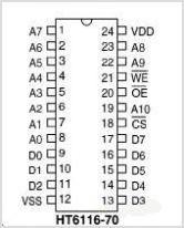
Without schematics it's going to be near impossible to find it :-(
But maybe it's just one broken trace and I can find it. I traced the
pin and it went to a 74LS373. I could replicate the above 'near fix' by shorting the pin on a 74LS373 logic chip to the pin next to it but
it only fixed the backgrounds and then the sprites had lines through them instead of the backgrounds.... the exact same fault I got when
piggybacking the RAM! I traced that RAM pin and it only went to that same 74LS373 logic chip I was shorting before, but it should be going
somewhere else as well because it's a RAM data pin. On PCBs data pins usually go to logic buffers and also to some other place where the
actual data originates. It must be a broken trace because it was only going to one place. Whatever else it is supposed to connect to is not
connected.
I decided to trace the pin next to the dead pin on the RAM and it joined to the same 74LS373 logic chip but also to a 74LS173 logic chip
near the sprite RAM on the other side of the board near the large sprite generator chip. I checked other pins on the RAM and there was a
pattern joining to the 74LS173 chip. I checked a different RAM and it went to another 74LS173 logic chip next to the first 74LS173 with the
same joining pattern but with one extra pin connected. Bingo!
The 4x 6116 RAMs are wired together so that 2x 8-bit RAMs make 1x 16-bit RAM where one RAM has D0-D7 and the other RAM has D8-D15. They are
basically wired together in pairs and it is very common to see this on arcade PCBs. On later boards 16-bit RAMs are joined in a similar way
to make a 32-bit or 64-bit RAM. By comparing the pattern I figured out that the suspect RAM was only connected on three pins with one pin
connection missing on the 74LS173 chip....
RAM (pin) -> LS173 (pin)
-----------------------
D7 (17) -> Q3 (6) <--- missing!
D6 (16) -> Q2 (5)
D5 (15) -> Q1 (4)
D4 (14) -> Q0 (3)
Here's the 74LS173 pinout....
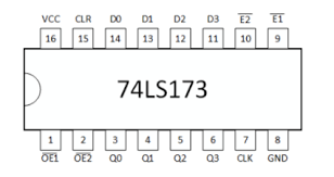
The Q0-Q3 pins are outputs and pin 6 on the 74LS173 was active and is supposed to be joined to the RAM. This is the missing trace!
I hooked up my micro-clips to see if that would fix it and....
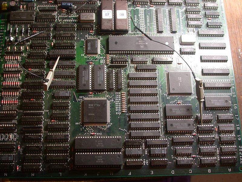
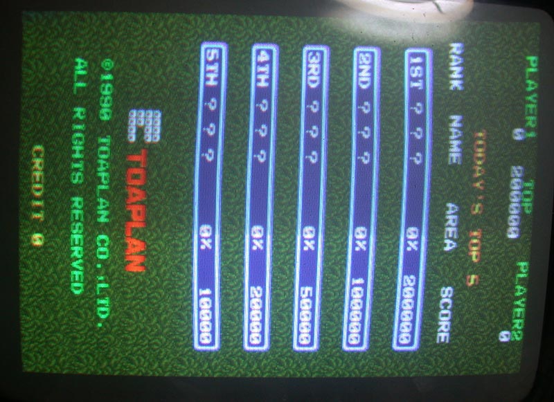
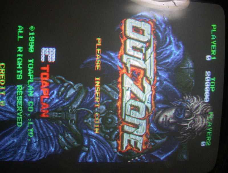
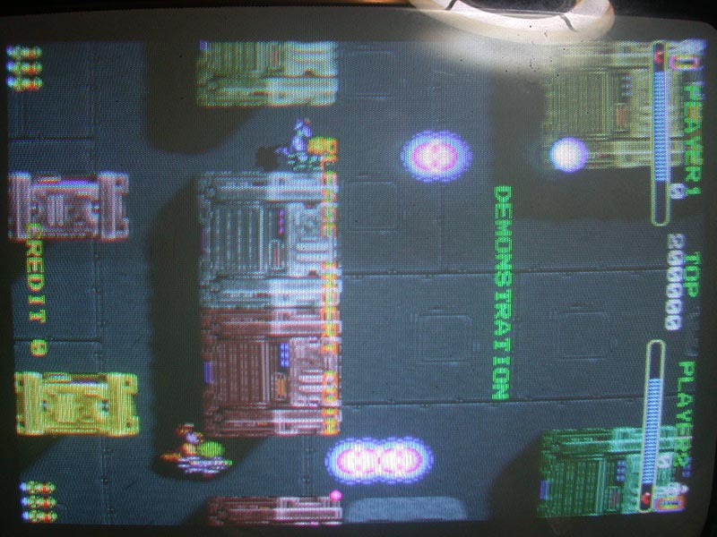
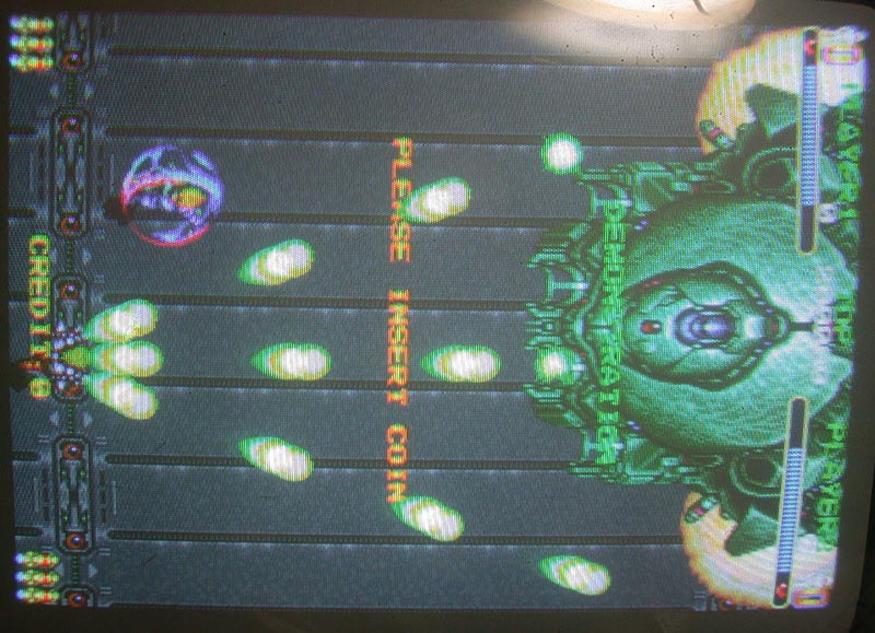
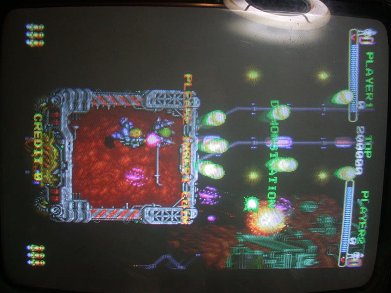
Yep! That was it!
Ok so now I need to find the actual broken trace and fix it properly, I don't want a bodge wire running across the PCB because that's just
nasty.
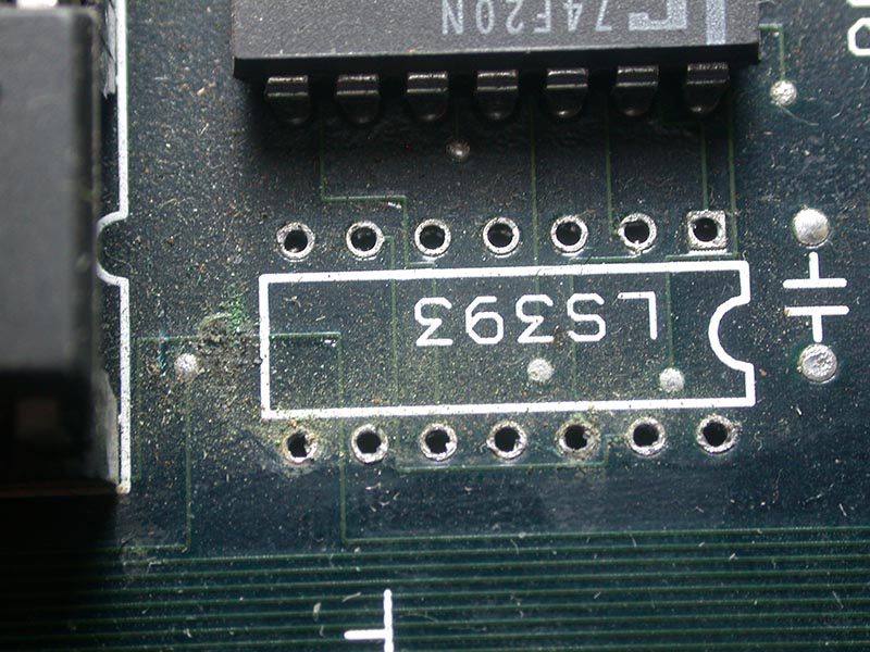
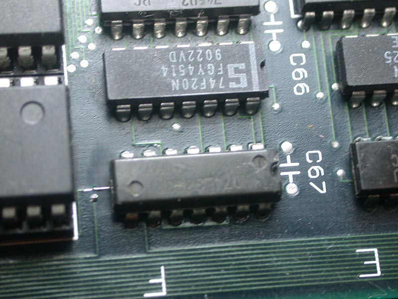
I traced back from the 74LS173 pin 6 and it went under a 74LS393 which had some minor corrosion. Probably this PCB was stored pooly in a shed
and water dripped on it at some point in the past and ate through a trace over the course of 10+ years. I removed the logic chip and then it
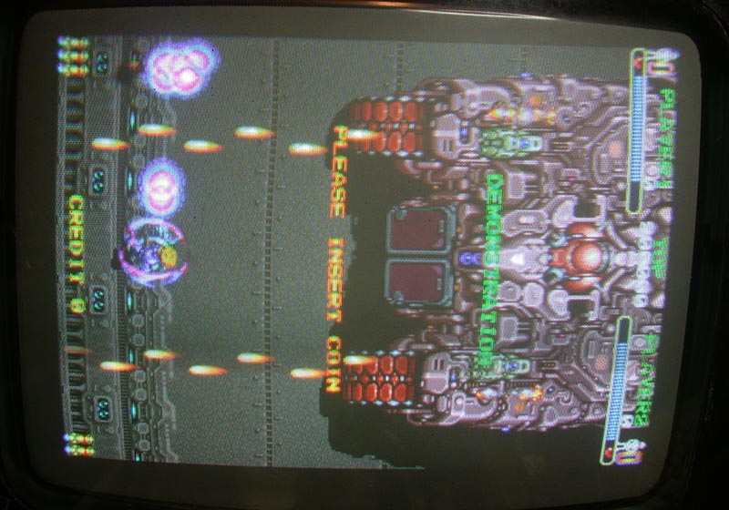
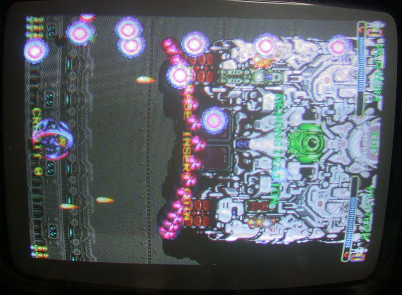
was pretty clear. I cleaned up the trace by removing the solder mask then soldered a small piece of wire across the
broken trace, put back the logic chip and that fully fixed it. The piece of patch wire is about 3mm long and 0.1mm diameter....

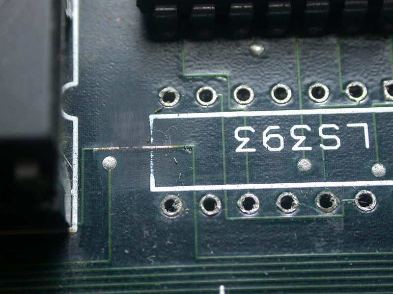


I put back the original mask ROMs, re-set the jumpers and everything was still working well so the ROMs were ok.
This would have been a lot easier with schematics! Hmmm, I wonder.... just for giggles I searched on the net not expecting to find anything
and wow, was I surprised what I found! Yep, schematics for Toaplan Outzone are available! D'oh!
Here's the relevant section showing how the 74LS373, 74LS173 and 6116 RAM connects, just as I have documented above.
The signal trace is named FY15....

Notice how this signal is connected with a single line to the other chips. This is called a bus and is used on a drawing to minimize having
to draw a lot of lines. In this case it's the data bus for the video mixing RAM. It takes data from all the ROMs and after being processed
by the graphics chips is sent to the 4x 6116 RAMs which go into another custom chip that does the mixing, sends that data to more RAM (for
color) and then out through some logic to the final R,G,B signals. Each signal is shown on the actual chip with the pin number as well
because they all share the same bus. The bus is not important, but the signals on the chips and the pin numbers are very important. This
becomes a big problem if the signal names and pin numbers are not readable (if the scan was done by some loser with a potato scanner) then
it makes the whole schematic useless. So remember, if you scan any schematics always make sure the signal labels on the chips are readable!
300DPI is a good base point, 600DPI is better, but always check it by zooming in to read the text. Fortunately in this case *most* of the
text is readable but rare schematics like these should have been scanned at a higher resolution.
Anyway, I suppose the moral of this is if you have a broken trace and it doesn't look too difficult you can figure it out with your brain,
but first make sure you search for a schematic just in case it's available because assuming it is readable it will save you a bunch of time
hehe!
|
|

